


Chips and Bits
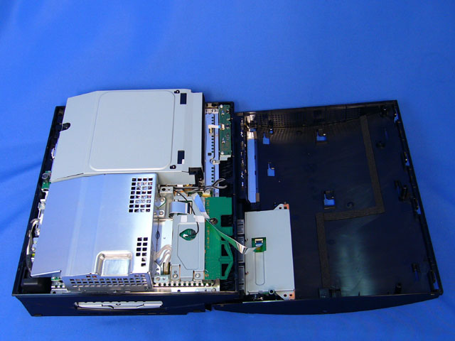
The PlayStation 3 is by far the most complex consoles to date, and a look at the inside reveals that the thermal design is even more complex than that of notebooks and desktops today. On the motherboard of the PlayStation 3, there are a few key elements on the motherboard that immediately attract the eye: the two most prominent being the Cell processor and RSX graphics engine.
More than five years in the making, the Cell Processor was developed jointly by Sony, Toshiba and IBM. The processor's name originated from the idea for a chip that operated in a similar fashion of a complex organism. Multiple 'cells' capable of general tasks, but all devoted to achieving a greater goal.
The Cell is a multicore chip capable of multi-threaded, massive floating point calculation. It comprises of a 64-bit PowerPC-based Power Processing Element (PPE) and eight identical Synergistic Processor Elements (SPE) running at 3.2GHz. The Cell consists of 234 million transistors and is manufactured on a 90nm silicon-on-insulator process.
The PPE is a dual issue, multi-threaded, in-order processor. It features a 64KB L1 cache, a 512KB L2 cache and shares many design cues with other PowerPC processors (this also gives it VMA/Altivec-like features). Most modern processors are of the out-of-order type, Cell forgoes this in favor of power savings and excessive transistor count. Being confined to its in-order architecture leads to decreased performance in applications with multiple branches, though clever programming, elegant compilers and the sheer speed of Cell may be able to minimize the downside. In essence, the Cell follows much of the RISC processor philosophy.
Each SPE is an independent, single precision, vector processor with 128 128-bit registers and four single precision floating point units. Each SPE is able to take a single instruction and perform multiple operations, just like how Intel used MMX or SSE technology to add SIMD (single instruction multiple data) to its Pentium CPUs. SIMD processor technology is ideally suited towards media applications such as games, movies and other forms of digital content.
The first six SPE's are dedicated to intense computational tasks. The seventh SPE is dedicated to OS security, and an eighth is included to help improve production yields by following the "baker's dozen" rationale (i.e., only seven out of eight cores need to be functional in order to be a approved for use in PS3). It is optimized for computational intensive workloads and media applications, such as games, movies and other forms of digital content.
Unlike the PPE and most modern day processors, the SPEs do not contain any cache whatsoever. Instead of cache, each SPE unit has 256KB allocated for local stores. While cache operates independent from programmer control, anything placed into an SPE's local memory must be explicitly planned by the programmer. The advantage of this is that it takes the unpredictability of cache out of the equation, which leaves room for greater performance. The disadvantage of this, of course, is that it takes the complexity away from the processor and puts it squarely on the shoulders of software programmers. This is one of the reasons that developers are commenting on the challenges of working on PlayStation 3. But with smart programming, storing to local memory will yield faster performance than using a general cache.
At this time, very little information about the NVIDIA RSX (Reality Synthesizer) processor is known, however we can pick some information out from the assembly. The RSX is a 550MHz graphics engine based on the G70 architecture, the same architecture family responsible for the GeForce 7800 series GPU. However, several reports indicate that the RSX is actually running at 500MHz core.
Four 512Mbit GDDR3 DRAM modules are integrated onto the RSX package, providing a total of 256MB of on-GPU memory. The chips in our console are Samsung modules rated at 700MHz (at least, according to the chip labels) which is essentially in-line with what reports claimed earlier this year. Like the original Xbox, the PlayStation 3 incorporates a memory controller on the graphics engine. According to documents leaked earlier this year, developers are supposed to use the RSX to access the main XDR memory or the GDDR3 memory found on the RSX chip.
256MB of Samsung XDR DRAM composes of the system's main memory. The memory on our console is listed at 400MHz, or 3.2Gbps. Also found on the console is a single 128MB Samsung NAND, signifying that the PlayStation 3 utilizes flash memory in some way.
Like the Xbox 360, the serial connections between the processor and GPU are easily visible, although the complexity on the PlayStation 3 is also apparent. Whereas the Xbox 360 essentially had two main controllers, the PlayStation 3 also adds two additional chips: the PlayStation 2 Emotion Engine and IO bridge (CXD2973GB). However, the Emotion Engine featured on the PlayStation 3 is more than just a die-shrink of the chip found on the previous generation console since the entire PlayStation 2 Graphics Synthesizer is also present on this chip; a feature present since the V9 PlayStation 2. What was an entire console in 1999 is now a single, passively cooled chip. A pair of Rambus DRAM chips is configured close to the EE/GS chip, similar to how they were found in the PlayStation 2.
Outside of Sony and NVIDIA, the company with the most chips in the PlayStation 3 is undoubtedly Marvell. Marvell has been a long time ally with Sony -- virtually all of the PSP networking and storage is provided by Marvell. The traces from the Ethernet port to the Marvell chip are also easily visible.
Thermals
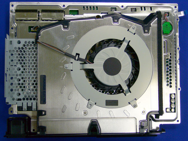
The PS3 is cooled by a single heatsink that covers a large majority of the motherboard. Under this heatsink, four more heatspreaders are revealed. Two of these heatspreaders house the Cell processor and the RSX.
Heatpipes dissipate heat from the Cell and the RSX along the system heatsink. This heatsink is cooled by a single 160mm fan with an exhaust along the back and sides of the console. The Cell processor is clearly the largest source of heat for the console, and it is situated directly underneath the 160mm fan. The Emotion Engine and
The entire power supply is built into the PlayStation 3. The Xbox 360 requires an external "brick" that can be swapped out depending on the local regulations for electronic devices. The
Additionally, the AC to DC step does not have any specific cooling on the PlayStation 3. Virtually all of the active cooling is handled by the single heatsink and fan on the other side of the backplate that houses the motherboard. It does not seem as though this upper half of the PlayStation 3 is hermetically-sealed, there appears to be very little airflow to the rest of the console here.
No comments:
Post a Comment